Amateur ExtraE7B11
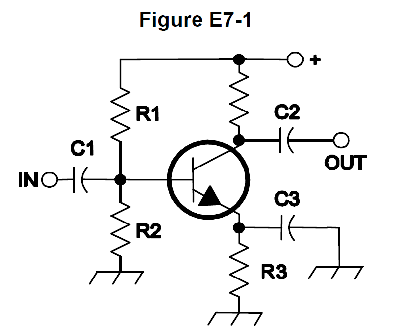
In Figure E7-1, what is the purpose of R3?
D
Answer
Practical circuits and system design
Type
A
Fixed bias
B
Emitter bypass
C
Output load resistor
D
Self bias
Answer Notes
In the standard transistor amplifier diagram (Figure E7-1), R3 represents the emitter resistor, located between the transistor's emitter and ground. As current flows through the transistor, it creates a voltage drop across R3. If the current tries to increase (due to temperature changes or varying transistor gain), this voltage drop increases, which raises the emitter voltage and consequently reduces the base-emitter voltage.
This negative feedback mechanism automatically stabilizes the transistor's operating point, a process known as self-bias or emitter bias. It prevents thermal runaway. It is not an emitter bypass (which would be a capacitor in parallel) or an output load resistor (which is usually on the collector).
Previous · E7B10
In Figure E7-1, what is the purpose of R1 and R2?
Next · E7B12
What type of amplifier circuit is shown in Figure E7-1?